Howdy, Stranger!
It looks like you're new here. If you want to get involved, click one of these buttons!

Quick Links
Nvidia's presentation was fairly shocking.
Either the rumored specs were off by a factor of two or else the presentation was extremely misleading to try to make it sound like the cards are twice as fast as they are. There isn't really any in-between here. Either the factor of two is there or it isn't, and either way is rather shocking.
I should explain. GPUs have a lot of different pieces, and there isn't just one number that you can point to and say, this is how fast the card theoretically should be across the board. There are a lot of things that you can compute from the paper specs, though. Arguably the most important is the card's computational power, the theoretical TFLOPS, or trillions of floating-point operations per second. It tends to be pretty strongly correlated with memory bandwidth, among other things, as if you took a balanced card and gave it four times as much memory bandwidth but no additional compute, you wouldn't make it much faster in most games, as the memory controllers would mostly be sitting there idle on such an unbalanced card. Similarly, if you gave it four times as much compute but no more memory bandwidth, the shaders would mostly sit there idle waiting on memory.
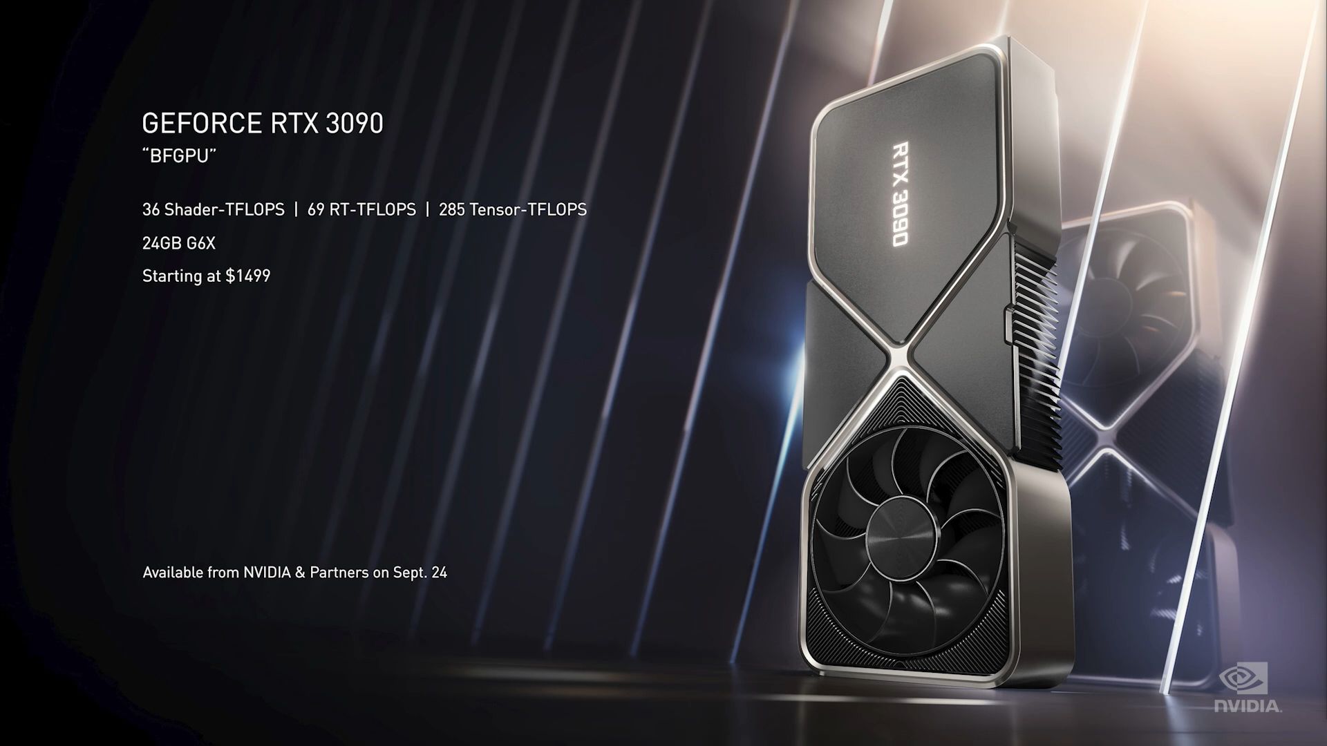
The leaked specs on the GeForce RTX 3090 from the box art of a new Gainward card is 5248 shaders and a 1.725 GHz boost clock. You can compute the theoretical TFLOPS from that as (number of shaders) * (clock speed) * 2, or 5248 * 1.725 * 2 * 10^(-9) ~ 18.1. So here's Nvidia's slide from their presentation:
https://images.anandtech.com/doci/16060/20200901173540.jpg
36 "shader-TFLOPS". That's double what you'd get from the computations. Card specs do sometimes change late. They don't change at the last minute by a factor of two. Rumors from random people making things up sometimes are off by a factor of two (remember the rumors that the mid-range GF104 was going to be a lot faster than the high-end GF100?), but it doesn't seem plausible that that is the case here.
So where did that factor of two come from? These aren't the only Ampere cards. Nvidia has already announced more specs for their A100 compute card of the same architecture. It has 6912 shaders at about 1.41 GHz, for 19.5 TFLOPS. I don't see where Nvidia explicitly states the shader count, but the TFLOPS number is here:
https://www.nvidia.com/en-us/data-center/a100/
It seems implausible that the rumored shader count is off by a factor of two, as that would mean that Nvidia packed in massively more shaders into a GeForce card than they did their A100 compute card that is the largest GPU ever built. Maybe I could believe that if the GeForce card chopped out a ton of compute stuff, but their presentation explicitly said that it includes the full tensor cores. The RTX 3080 is listed as 28 billion transistors, or only a little over half of what the A100 uses.
It also seems implausible that the clock speed is off by a factor of two. GPUs tend to clock a little under 2 GHz these days for reasons of physics, and if they suddenly tried to clock a huge GPU at 3.5 GHz, that's not going to end well.
Most likely, the factor of two is that instead of a * 2 in the computations, they did a * 4 instead. But why?
At this point, it's very reasonable to ask, why should there be a * 2 at all? The answer to that is that all shaders can do one fma per clock, where fma(a, b, c) = a * b + c, all as 32-bit floats. An add is one operation and a multiply is another, so being able to do both at once per clock counts as two. Yeah, that's fishy, but all modern GPU vendors do it, so it at least gives you comparable numbers.
Did Nvidia add some other operation that they think should count as four? The most obvious candidate would be packed half math. That is, rather than putting a 32-bit float in a 32-bit register, you pack two 16-bit halfs in, with a 16-bit number in the high 16 bits and a completely independent 16-bit number in the low 16 bits. Then you have an operation that can do an fma on the high 16 bits and another fma on the low 16 bits at the same time. So that counts as four. But it's not four 32-bit operations. It's four 16-bit operations. This is why GPUs will commonly site one number of TFLOPS at 32-bit precision, and another number at 16-bit. See here, for example:
https://www.amd.com/en/products/professional-graphics/instinct-mi50
6.6 TFLOPS double precision
13.3 TFLOPS single precision
26.6 TFLOPS half precision
53 TOPS int8 precision
It takes two 32-bit registers for a 64-bit number. But that 32-bit register can have a full 32-bit float, two 16-bit halfs, or four 8-bit integers. It's no coincidence that halving the data size doubles the throughput, at least if the card has the logic for it, as AMD's Vega 20 does.
But if some other operation is the culprit, why didn't they count it in their A100? Furthermore, the ratio of various operations is dictated by the architecture. If you add twice as many compute units, you get double the throughput of everything. Increase the clock speed by 10% and you get 10% more throughput of everything. The A100 cites peak 312 TFLOPS half precision from tensor cores (= 19.5 TFLOPS single precision * 16), with the 16 having a factor of 2 because of half precision times a factor of 8 because the tensor cores use 8x8 matrices.
I should explain. GPUs have a lot of different pieces, and there isn't just one number that you can point to and say, this is how fast the card theoretically should be across the board. There are a lot of things that you can compute from the paper specs, though. Arguably the most important is the card's computational power, the theoretical TFLOPS, or trillions of floating-point operations per second. It tends to be pretty strongly correlated with memory bandwidth, among other things, as if you took a balanced card and gave it four times as much memory bandwidth but no additional compute, you wouldn't make it much faster in most games, as the memory controllers would mostly be sitting there idle on such an unbalanced card. Similarly, if you gave it four times as much compute but no more memory bandwidth, the shaders would mostly sit there idle waiting on memory.
The leaked specs on the GeForce RTX 3090 from the box art of a new Gainward card is 5248 shaders and a 1.725 GHz boost clock. You can compute the theoretical TFLOPS from that as (number of shaders) * (clock speed) * 2, or 5248 * 1.725 * 2 * 10^(-9) ~ 18.1. So here's Nvidia's slide from their presentation:
https://images.anandtech.com/doci/16060/20200901173540.jpg
36 "shader-TFLOPS". That's double what you'd get from the computations. Card specs do sometimes change late. They don't change at the last minute by a factor of two. Rumors from random people making things up sometimes are off by a factor of two (remember the rumors that the mid-range GF104 was going to be a lot faster than the high-end GF100?), but it doesn't seem plausible that that is the case here.
So where did that factor of two come from? These aren't the only Ampere cards. Nvidia has already announced more specs for their A100 compute card of the same architecture. It has 6912 shaders at about 1.41 GHz, for 19.5 TFLOPS. I don't see where Nvidia explicitly states the shader count, but the TFLOPS number is here:
https://www.nvidia.com/en-us/data-center/a100/
It seems implausible that the rumored shader count is off by a factor of two, as that would mean that Nvidia packed in massively more shaders into a GeForce card than they did their A100 compute card that is the largest GPU ever built. Maybe I could believe that if the GeForce card chopped out a ton of compute stuff, but their presentation explicitly said that it includes the full tensor cores. The RTX 3080 is listed as 28 billion transistors, or only a little over half of what the A100 uses.
It also seems implausible that the clock speed is off by a factor of two. GPUs tend to clock a little under 2 GHz these days for reasons of physics, and if they suddenly tried to clock a huge GPU at 3.5 GHz, that's not going to end well.
Most likely, the factor of two is that instead of a * 2 in the computations, they did a * 4 instead. But why?
At this point, it's very reasonable to ask, why should there be a * 2 at all? The answer to that is that all shaders can do one fma per clock, where fma(a, b, c) = a * b + c, all as 32-bit floats. An add is one operation and a multiply is another, so being able to do both at once per clock counts as two. Yeah, that's fishy, but all modern GPU vendors do it, so it at least gives you comparable numbers.
Did Nvidia add some other operation that they think should count as four? The most obvious candidate would be packed half math. That is, rather than putting a 32-bit float in a 32-bit register, you pack two 16-bit halfs in, with a 16-bit number in the high 16 bits and a completely independent 16-bit number in the low 16 bits. Then you have an operation that can do an fma on the high 16 bits and another fma on the low 16 bits at the same time. So that counts as four. But it's not four 32-bit operations. It's four 16-bit operations. This is why GPUs will commonly site one number of TFLOPS at 32-bit precision, and another number at 16-bit. See here, for example:
https://www.amd.com/en/products/professional-graphics/instinct-mi50
6.6 TFLOPS double precision
13.3 TFLOPS single precision
26.6 TFLOPS half precision
53 TOPS int8 precision
It takes two 32-bit registers for a 64-bit number. But that 32-bit register can have a full 32-bit float, two 16-bit halfs, or four 8-bit integers. It's no coincidence that halving the data size doubles the throughput, at least if the card has the logic for it, as AMD's Vega 20 does.
But if some other operation is the culprit, why didn't they count it in their A100? Furthermore, the ratio of various operations is dictated by the architecture. If you add twice as many compute units, you get double the throughput of everything. Increase the clock speed by 10% and you get 10% more throughput of everything. The A100 cites peak 312 TFLOPS half precision from tensor cores (= 19.5 TFLOPS single precision * 16), with the 16 having a factor of 2 because of half precision times a factor of 8 because the tensor cores use 8x8 matrices.

![[Deleted User]](http://w8.vanillicon.com/v2/8187bdfebcad0c6fe557549abc3ef848.svg)


Comments
So maybe they cited a half precision TFLOPS number and tried to make you think it's single precision? But they're also claiming 1.9x performance per watt as compared to Turing. For obvious reasons, you shouldn't compute performance per watt by comparing floats on one architecture to half precision on another.
Let's look at a GeForce RTX 2080 Ti, for comparison. As a long released card, it's specs are well-known: 4352 shaders, 1.545 GHz, 13.4 TFLOPS. With a TDP of 250 W, you can compute a theoretical efficiency of 53.8 GFLOPS/watt. Plug in the rumored 350 W TDP for the RTX 3090 and you get 51.7 GFLOPS/watt. Thus, on paper, the RTX 3090 has 0.96 times the energy efficiency of a GeForce RTX 2080 Ti. But Nvidia's claim of 1.9 times the efficiency is double that, and again, we're off by a factor of 2.
Nvidia did not give power numbers today, and that 350 W would be by far the highest for a single GPU card ever, at least if you exclude the 400 W from that A100 compute card. So on the surface, it's plausible that the real power consumption is less than 350 W, and possibly a lot less. If it were 175 W, that gives you 1.9x energy efficiency. And while there have been a lot of GPUs that used around 175 W, such as the GeForce RTX 2070, you don't create a new 12-pin power connector when a single 8-pin one would have been good enough. Zotac's leaked version of the RTX 2090 has three 8-pin power connectors. Two would let the card use 375 W while at least having the power draw per connector stay in spec, though the PCI Express specification has a maximum board power of 300 W that is sometimes ignored.
Now, the 1.9x energy efficiency would be true if you're only counting tensor operations. Ampere does 8x8 matrices while Turing did 4x4 matrices, so Ampere has double the tensor throughput per shader. It might even be true if you're only counting ray-tracing operations. There could be plenty of shenanigans there as to what count as how much, but it is very plausible that Ampere does ray-tracing a lot better than Turing, and the rumored 2x as well per shader wouldn't be a surprise.
But if that's all that is going on, with a 1.9x performance increase in tensor cores and ray-tracing but decreasing efficiency of everything else, then trying to claim that's typical of gaming is a straight-up lie. Maybe lawyers vetted it and decided that they could justify it in an arcane sense just barely well enough for the claim to not quite be securities fraud, but in common English, that would be a straight up lie. Which is why I say that it would also be shocking if that's the case.
Good thing there will be independent reviews. Wait for the reviews and don't put in a pre-order ahead of time.
For comparison RTX 2080 Ti has 4 352 CUDA cores. It looks like NVidia really doubled the FP32 performance, and those previous rumors were off by factor of two.
https://www.nvidia.com/en-us/geforce/graphics-cards/30-series/?nvid=nv-int-csfg-14125
Which is interesting, but makes me ask, 2x as compared to what? What about other instructions? How hard is it to use it? What's the catch? Because I don't believe that they can just double throughput without a catch.
I'm reminded of AMD's old VLIW architectures where an AMD GPU indeed had much higher theoretical TFLOPS numbers as compared to an Nvidia GPU of comparable performance. The catch was that a given work unit had to do five of the same operation at the same time, quite apart from the different work-items in a warp needing to stay together as GPUs normally do. That made it so that you couldn't come anywhere near maxing out the theoretical throughput except for a handful of very special cases.
But that isn't a negative comparison. AMD's approach at the time was, yeah, it's hard to use all of our shaders at once. But we have so many of them that we still win, as you had a Radeon HD 4870 with 800 shaders competing against a GeForce GTX 260 with 192 shaders. If Nvidia came up with some trick that doubles the theoretical compute available while "only" letting you use 1.5x as much as before, that's still a big win.
My best guess is that in Turing, they said that you could do integer and floating-point operations at the same time. At the time, I said, that's dumb. You usually don't want to do integer and floating-point at the same time. Most GPU workloads are either very heavy on floating-point with very little integer (mainly memory addressing, and even some of that can be floating-point) or else almost purely integer with little or no floating-point at all. So why make it so that you can do two things at once that you don't want to do at the same time? If you can do an operation from set A and one from set B at the same time, why not mix the operations better so that it will be common to want about half from each set?
Well, maybe they decided to just put floating-point fma in both halves, and leave everything else as being in at most half of the shaders. For graphics, that might well be a win, and without eating up stupid amounts of die space. But it will depend tremendously on the details of how hard it is to use. Architectures that tried to get too fancy have botched that before; Kepler comes to mind. Reviews will be interesting.
With GTX 1000 -generation NVidia's shaders had to choose between doing FP operations or INT operations (FP = floating point. It means decimal number. INT = integer). In RTX 2000 -generation NVidia introduced separate datapaths for FP and INT operations so that integer operations did not slow FP operations down so much.
With RTX 3000 -generation NVidia has gone back on that change, and their shaders again have to stop FP operations when doing integer calculations. It means a TFLOP of FP32 -performance for RTX 3000 should be a bit slower than it was for RTX 2000 -generation, but RTX 3000 should be comparable to GTX 1000 which used similar solution.
Additionally, NVidia has gone and removed integer capacity from half of their shaders completely. The new generation will have 50% shaders that will be able to switch between FP and INT calculations, and 50% shaders that can only do FP calculations.
This sounds like a brilliant move because when doing graphics the cards will mostly do FP -calculations. It likely allowed NVidia to use a lot less transistors per shader without any speed drop in games, and consequently pack a lot more shaders to the card.
https://www.reddit.com/r/nvidia/comments/iko4u7/geforce_rtx_30series_community_qa_submit_your/
Search for answer to question by redsunstar
Nvidia sure botched their Turing architecture. But other than doubling down on tensor cores, they seem to have realized it and gone back to what worked better in Maxwell/Pascal. It wasn't a terrible architecture overall, but what they did with shaders makes you ask how anyone could conceivably think that was a good idea.
For the sake of simplicity, I'm going to ignore warps and just talk about the two shader banks within a partition of a compute unit as "cores". Yes, I'm well aware that each of my "cores" here has 16 shaders, takes two clock cycles to start the same instruction for 32 work-items in a warp, there are four partitions in a compute unit, a lot of compute units, also special function units sitting around somewhere, and so forth. But let's ignore that for now.
The way that Nvidia GPUs have worked for the last several generations is that you have pairs of cores with different instructions in them. Each thread gets assigned to a particular pair of cores. There are many such pairs of cores on the whole GPU, but each thread is on one particular pair of cores. The two cores in a pair are not identical, but can have different instructions. There can actually be a lot of threads assigned to the same pair of cores, but a thread never gets moved to other cores.
The idea is that as your program executes, on every clock cycle, the schedulers will try to pick the next instruction available from one of the threads assigned to a pair of cores and execute it on the core that the scheduler is assigned to. It is fully in-order execution, so the order of instructions for a single thread is chosen at compile time and not rearranged later. What makes scheduling very different from a CPU is that there can be many threads on the same pair of cores at the same time, and every clock cycle, it picks the next instruction from some thread and schedules it, but it can switch which thread every clock cycle.
If an instruction is available in both of the cores, then it can be executed on either core. If it is only available in one of two cores that the thread has available, then it must be scheduled on that particular core. Often, the core that doesn't have the instruction that a particular thread needs will have the instruction that some other thread needs, so that other thread uses the other core.
The more instructions you put into a core, the larger and more expensive that core is. Bigger, more expensive cores mean that you can't have as many of them on a chip. So it is efficient to not just put all instructions into all cores. In order to be a fast instruction, it has to be available in at least one of the two cores (other, slower instructions are also available in special function units, but let's ignore that). But ideally, you want your cores to be such that if a problem is limited by compute, most of the time, both cores can execute something in pretty much every clock cycle. And you want the cores to be as small and cheap as possible while still having enough to usually be able to execute something.
In graphics, most of the instructions are floating-point arithmetic. More specifically, add, multiply, or fma, where fma(a, b, c) = a * b + c. Obviously, if you can do fma, you can add or multiply. But there are some other instructions used, such as integer arithmetic, exponentials, logarithms, trig functions, and so forth. If you want to keep both cores busy most of the time in games, then what you do is to put fma in both cores, and maybe some other common, cheap things. But for most instructions, just one core or the other is enough. Maybe you'd like to balance them such that some of the other instructions go in one core and others go in the other core, but you don't need to lay out the space to put the instruction in both.
That's usually what Nvidia has done over the years. Sometimes some cheap integer instructions were in all of the cores and sometimes not. But you always put floating point add, multiply, and fma in both, as those are your workhorses. Tesla did that, Fermi did it, Kepler did, Maxwell/Pascal did, and now Ampere does. For that matter, all AMD GPUs ever made (at least launched since they bought ATI in 2006) do.
Volta/Turing didn't, and as far as I'm aware, that's the only GPU architecture ever that didn't, at least in the programmable shader era that dates to about the turn of the millennium. (Some very old 2D video cards probably didn't have floating-point at all.) Instead, for some inexplicable reason, Nvidia decided to put the integer instructions into one core and the floating-point instructions into the other. As a way to partition instructions into cores, that's egregiously dumb. You want both cores to be in use at the same time. Nvidia marketing tried to advertise this as a good thing, in that now you could do both integer and floating-point instructions at the same time without one taking away from the other. But it effectively did so by making them both half speed.
The problem is that basically nothing is about half integer and half floating-point. Games are very floating-point heavy, so most of the computations needed use floats. Even algorithms that do have a lot of integer work tend to be mostly or entirely integer, with little to no floating point. For example, I'd bet that more than a few cryptocurrency mining programs never have a single float touch the GPU at all. So that partition means that you can rarely keep both cores busy very much of the time. And the whole goal here is to keep both cores busy most of the time.
Nvidia did decide to count the pair of cores in Volta/Turing as a single core for marketing purposes. Thus, a GeForce RTX 2080 Ti with 4352 pairs of cores is marketed as having 4352 shaders, while a GeForce GTX 1080 Ti with 1792 pairs of cores is marketed as having 3584 shaders. I'm not criticizing the latter decision. Nvidia probably could have said that the RTX 2080 Ti had 8704 shaders if they wanted to. But that would have made it obvious that something was wrong, if Turing had 2.43 times as many shaders but was nowhere near 2.43 times as fast.
Of course, CUDA cores are rarely the sole bottleneck in GPU performance, which is why overall GPU perf doesn't scale up by the number of CUDA cores. Essentially the ratio of FP32 ALUs:ROPs and ALUs:TEX has been doubled
But it does mean that INTs will cut into your FP throughput once more, assuming that you could schedule enough FP work to keep both math pipes busy
It also means that there's now a very fixed ratio between the raster engines and ROPs. You can't disable one without disabling the other
The payoff here is that you no longer need to ramp up the core voltage just because the MCs need more power, or vice versa. It's finer-grained power control
enabled for all GA10x GeForce parts
Sparsity is a great feature. But I wish NVIDIA had been clearer about this in Tuesday's presentation. For reference, for Big Ampere at GTC they were always reasonably clear on this point